by Mike Donnelly
15 March 2021
In my previous article, I introduced the new BCI ROM export capability from Simcenter Flotherm. These accurate thermal models run directly in PartQuest Explore and simulate orders of magnitude faster than the full 3D/CFD analyses of the systems they represent. This is important for running transient simulations with long end-times that are needed for temperatures to reach steady-state.
These models work well for electro-thermal simulation, as long as the “electrical” aspect of the system also simulates quickly over those long virtual operating times. This was the case for the two examples I chose for that article; an abstract model of a “Digital Smartphone” with Dynamic Thermal Management, and an analog (linearly regulated) “LED Spotlight” with over-temperature protection. But this is not the case for a very important class of electronics: Switching Power Circuits.
The problem with electro-thermal simulation of switch-mode circuits
Figure 1: Buck 12V to 5V, 2A converter, switching at 400 kHz
Switching circuits frequently require long simulation run-times (i.e. wall clock time), even for relatively short simulation end-times. This is because practical switching frequencies are high (and getting higher), and for each switching cycle the simulator must solve a large set of simultaneous coupled non-linear differential equations, requiring many small time-steps. These short steps are needed to accurately resolve all of the fast-changing voltages and currents in the circuit. Even for the relatively simple Buck Converter example of Figure 1, it takes 6 seconds to simulate just 1 millisecond of “virtual operating time”, or 6000 times longer than “real-time”. Running that simulation for hundreds or thousands of seconds of “virtual operation” is just not practical.
Note that the example in Figure 1 is a “Live” tunable design, which means that you can change the parameter values of the components highlighted in blue and run new simulations. For example you can change the input voltage level, or the fixed or the switched load resistor value, to see the effect on the transient response of the circuit.
The current waveforms in the lower left wave-scope show the negative transient “reverse recovery” behavior of the diode. This level of detail or fidelity of the component models is needed to not only accurately assess electrical performance of the circuit, but also for the accurate power dissipations needed to predict electro-thermal performance. This is described in more detail in the section “The need for In Situ Calibration” below.
A common circuit abstraction that is widely used for switching power converter control-loop design and analysis is the “state-average” modeling method, as shown in Figure 2 for the same Buck Converter. In this approach, the effective “average” state of the switched voltages and currents are used to model the conversion ratio between the input and output sides of the converter. These relationships can be expressed using ideal math multiply function blocks.
Figure 2: Ideal “state-average” model of the buck converter in Figure 1
Because there is no actual switching, the simulation speed of a state-average circuit can be many orders of magnitude faster than its switching equivalent. While the transient response and main operational behavior is comparable to the switching circuit, the simulation run-time for the state-average model is usually quite acceptable for the long settling times required for electro-thermal simulation.
The problem with the state-average model for electro-thermal simulation is that many of the components that generate heat (i.e. the switching components) are no longer part of the electrical circuit! Since the BCI ROM-based “thermal network” needs to know the power dissipation of each individual component, not only to predict its internal “junction” temperature, but also because of the location-dependence of each of these power-sources on the PCB. Therefore we must include the operating-point dependent heat flows for all the important power dissipating components in the original switching circuit.
A solution for electro-thermal simulation of switch-mode circuits
To address this problem, a 2-step modeling approach is demonstrated in this section. Step 1 is to calibrate the individual component losses under a range of circuit operating conditions. This calibration is performed on the actual switching circuit (i.e. “In Situ”), rather than on these components in isolation, so that any interactions that may affect the power dissipation of each component can be accounted.
Figure 3: “In Situ” electro-thermal calibration of the switching buck converter
The calibration test set-up for the Buck Converter shown in Figure 3 samples the power dissipation of the 3 key power stage components (i.e. the MOSFET, Diode and Inductor) over multiple operating states. The “In Situ Calibration” model in the upper left of the schematic, steps the operating conditions of the circuit in user-specified nested loops over time:
- The load current steps through 4 values, from 0.5A to 2.0A
- The input voltage steps through 3 values, 7V, 12V and 15V
- The power device operating temperatures step through 3 values, -40C, +25C and +150C
Combined, they give 36 different operating states. After a user specified settling time at each state, that model samples the average power dissipation over the last 10 switching cycles. These sampled average power dissipation values are shown as wave-scope graphs on the far left side of the schematic. Each x-axis “index” value (0 to 35) corresponds to one particular state. These sample sets are then downloaded as a .csv data file, for use in the next step.
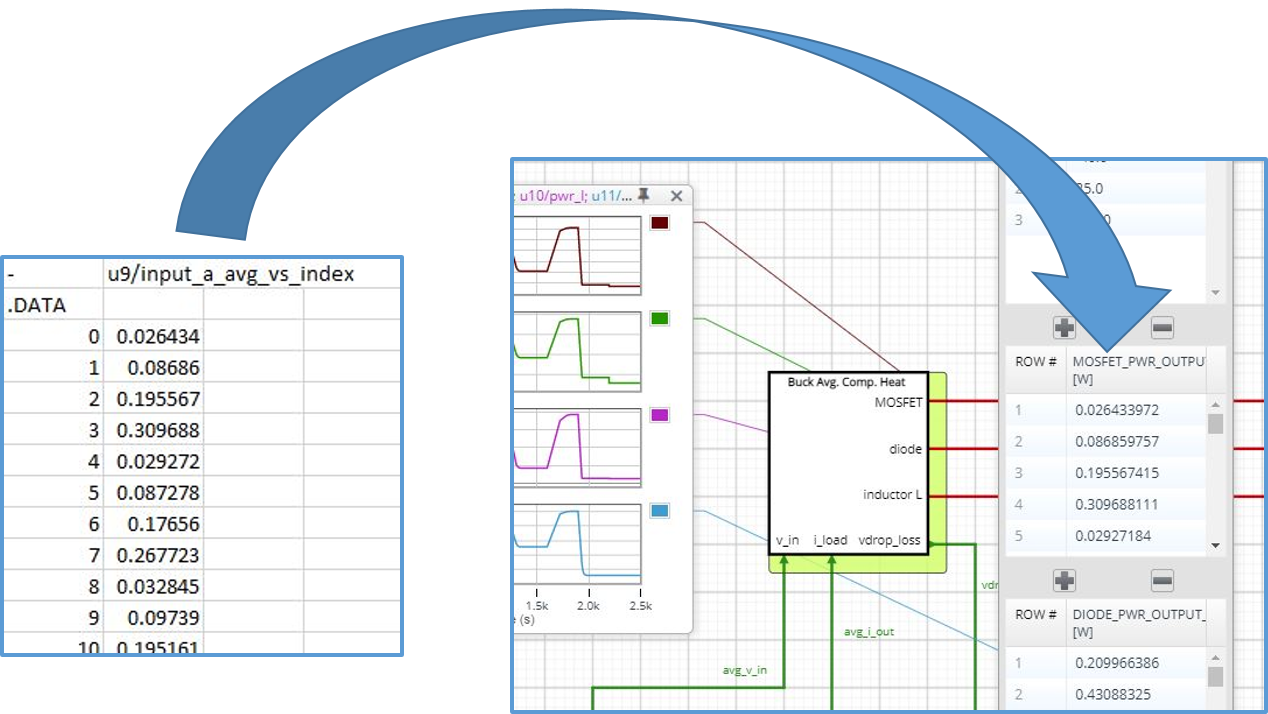
Figure 4: Copy/paste data from the calibration model into a tri-linear interpolation model
In Step 2, the data from the in situ calibration test is used in a tri-linear interpolation model placed in an electro-thermal state-average model of the converter. The data is simply copied from the downloaded waveform (.csv) file from Step 1, and pasted into the interpolation model as shown in Figure 4. That model is labeled “Buck Avg. Comp. Heat”. It is specific to this application, so the annotations and property values can be easily understood, but it can be extended to cover more general use-cases. It provides the average output power for each of the power stage components using a fast interpolation calculation, based on the three independent inputs (i.e. the instantaneous state-average values of the load current, input voltage and each component’s temperature).
Figure 5: State-Average electro-thermal model of the buck converter
When used with a state-average model of the buck converter, as shown in Figure 5, the tri-linear interpolation model provides the necessary time-varying power dissipation for each component, as the operating conditions change during a transient electro-thermal simulation. This provides the correct heat flow input values to the BCI ROMs of the components. These component thermal models are in turn connected to the BCI ROM of the full PCB, which includes the self- and cross-heating of all the power converter components, as well as the “processor”. That processor model presents a realistic “digital power” load to the converter (i.e. a clock frequency, voltage and operating-state dependent power demand).
Because the circuit in Figure 5 is “Live”, you can try changing the input or output set-point voltages, as well as any of the thermal heat-transfer Rth values on the BCI ROMs. Note that if a junction temperature exceeds 150 degC, that model is no longer in its calibration range. That component’s loss prediction is no longer sensitive to temperature, so it may give an inaccurate performance prediction.
The need for “In Situ” Calibration
As discussed previously, diode reverse recovery is one of the complex device behaviors that can impact both the electrical and thermal characteristics of a circuit. The presence of a reverse current in the diode when the MOSFET is first turning ON, results in an equal positive transient current pulse in the MOSFET, in addition to the full load current that is expected to be present. This additional current can be high enough to stress the MOSFET, and is always an important consideration in power electronics design. But that current can also contribute to unexpected additional heat input to the system.
Figure 6: Stand-alone calibration of MOSFET switching losses
The circuit in Figure 6 is configured to calibrate the switching losses of the MOSFET used in the Buck Converter. This circuit has an ideal load current source that is swept over a wide range, and an ideal diode (with no reverse recovery effect) to carry the current when the MOSFET switches OFF. The specialized “Switching Loss Measurement” model can detect the beginning and end of each switching interval, both for turning ON and turning OFF. It measures the “before” vs. “after” energy change and creates the waveforms shown in the wave-scope in the upper left, switching loss vs. load current.
The cursor indicates that at a load current of 2A (and input voltage of 12V), the turn-on energy per switch cycle is 142.8 nJ, and for turn-off it is 73.5 nJ. Since the Buck Converter switches at 400 kHz, the expected power loss due to switching would be 400 kHz * (142.8nJ + 73.5nJ) = 86.5 mW. In addition, for the 12Vin/5Vout conversion, the switching duty cycle would be 5/12 = 0.4167. When conducting 2A, and with the nominal Rds-on for the MOSFET of 0.07 Ohms, the expected conduction power loss would be 0.4167 * 0.07 Ohm * (2A)^2 = 116.7 mW. The expected total MOSFET power loss would be 116.7 mW + 86.5 mW = 203.2 mW.
But from the in situ calibration results at those same operating conditions, the measured (simulated) power loss was 305.3 mW. You can see this as the value of the cursor, at x-axis index = 19, on left-side wave-scope of Figure 3. This is a 50% increase from the “expected” MOSFET power loss, based on its measurement in isolation. This difference is in part due to the interaction with the diode’s reverse recovery behavior, but other factors may be contributing.
Alternate uses for in situ power loss modeling
A perhaps subtle but important benefit of having access to all the operating-state dependent component losses in the converter, is that that loss can represent a “non-ideal” characteristic in the otherwise ideal state-average model. Inside the “Buck Avg. Comp. Heat” model, the sum or total power loss for the three switching components is divided by the instantaneous average output current. This calculation gives an “effective” average voltage drop (“vdrop_loss”) that is placed in series with the converter output. In that simple way, an operating-state dependent loss factor is included in the state-average model. This method could be useful for “electrical-only” applications of state-average modeling, independent of the need for electro-thermal simulation.
The calibration data exported from the high fidelity switching circuit can also be imported into other design tools, including Simcenter Amesim, where it can be used in higher level system simulations.
More on trilinear interpolation
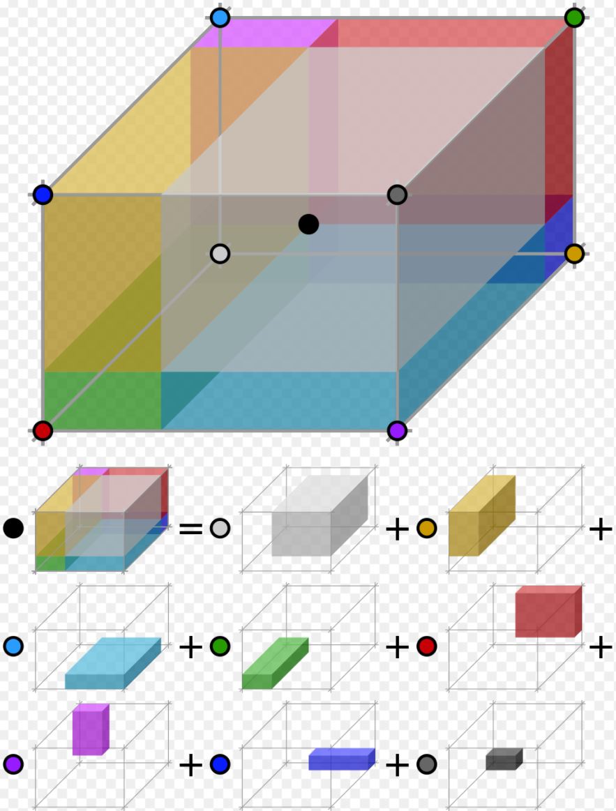
Figure 7: Geometric visualization of tri-linear interpolation
The geometric visualization of the trilinear interpolation calculation is shown in Figure 7 (Ref. Trilinear Interpolation, Wikipedia). It scales the 8 adjacent “corner” sample values to compute the function value at the internal interpolation point. The scale factors are proportional to the partial volumes diagonally opposite the corner being scaled.
Summary
This article describes an approach for using accurate BCI ROMs for electro-thermal simulation, in the challenging application of switching power circuits. That is, when state-average circuit models are needed to achieve practical simulation run-times. The approach, in situ calibration, preserves operating condition dependence and heat-source location awareness within that state-average model.
- 1811 views